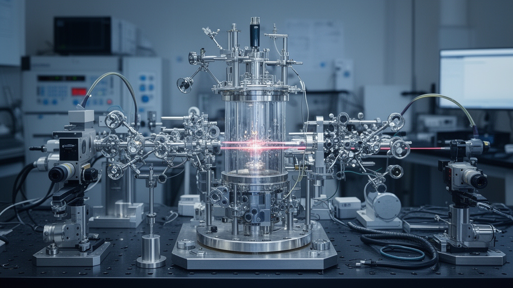
MIT researchers have unveiled a groundbreaking AI model that allows for 3D analysis of crystalline materials, a leap forward in understanding and engineering advanced substances which impacts fields ranging from manufacturing to sustainable product design. By automating the interpretation of complex diffraction patterns, this system provides a ‘crystal clear’ view of atomic structures that were previously nearly impossible to map in three dimensions without months of manual labor. This development marks a pivotal shift in materials informatics, turning a bottlenecked process into a high-speed engine for discovery.
The Mechanics: Decoding the Atomic Lattice
At the core of the challenge in materials science is the characterization of crystalline structures. Most materials, including semiconductors, battery cathodes, and high-performance alloys, rely on specific atomic arrangements to define their properties. Scientists typically use Transmission Electron Microscopy (TEM) to view these materials. However, TEM provides 2D snapshots of 3D structures. To derive the 3D lattice structure, researchers traditionally had to perform complex, manual diffraction analysis—a process prone to human error and immense time consumption.
The new MIT-developed neural network bypasses this traditional manual interpretation. By training on vast datasets of simulated and experimental diffraction patterns, the model has learned to instantly recognize the relationship between 2D projection data and the actual 3D orientation of the crystal lattice. When presented with a 2D diffraction pattern, the AI can now reverse-engineer the 3D structure with a level of accuracy and speed that was previously unattainable, effectively unlocking the ‘internal blueprint’ of the material.
Transforming Materials Informatics
This breakthrough represents a massive jump in the field of materials informatics. Previously, characterizing a new material could take doctoral students or senior researchers days, if not weeks, to complete accurately. This process now occurs in seconds or minutes. The implications for the ‘Materials Genome’—the collective knowledge of atomic-level material properties—are immense.
With this tool, laboratories can now process thousands of material samples in the time it once took to process a handful. This capability allows researchers to screen for defects, identify novel phases, and optimize material composition in real-time. Whether it is identifying microscopic cracks in a new turbine blade or mapping the lattice integrity of a high-capacity battery material, the speed of this AI provides an unprecedented competitive edge in material development.
Real-World Applications: From Batteries to Semiconductors




The utility of this AI extends far beyond theoretical research. In the semiconductor industry, where atomic-level precision is the difference between a functional chip and a failure, this technology offers a robust method for quality control. Manufacturers can utilize this AI-driven characterization to ensure the uniformity of crystalline structures across wafers, drastically reducing waste and increasing yield.
Furthermore, in the transition toward sustainable energy, this technology is critical. Developing high-efficiency batteries requires understanding how ions move through the crystalline structure of cathodes. By using the AI model to quickly characterize these structures, engineers can iterate on battery designs faster, testing various chemical compositions to maximize energy density and longevity. Similarly, in the development of photovoltaic materials for solar cells, the AI assists in identifying crystalline orientations that yield the highest conversion efficiency, directly impacting the economic viability of green energy technologies.
The Future of Automated Laboratories
Looking ahead, this AI model is poised to become a central component of fully autonomous laboratory systems. Integration with robotic handling of samples could enable a ‘closed-loop’ research environment. In this vision, a robot prepares a sample, an electron microscope images it, the AI characterizes the crystal structure, and a secondary management system adjusts the synthesis parameters for the next batch—all without direct human intervention. This cycle of continuous improvement is the ‘holy grail’ of scientific research and represents a move toward the industrialization of material discovery.
Addressing Scientific Bottlenecks
One of the most significant aspects of this research is how it addresses the ‘data bottleneck’ in materials science. While we have the technology to generate massive amounts of data through imaging, the ability to make sense of that data has lagged. By providing an automated, high-fidelity interpretation engine, the MIT team has effectively ‘unclogged’ the pipeline. This research confirms that the future of materials science will not just be about better microscopy, but about better computation.
FAQ: People Also Ask
Q: How does the AI know the 3D structure from a 2D image?
A: The AI model is trained on ‘synthetic diffraction data.’ It learns the mathematical relationship between 2D diffraction patterns (the patterns light or electrons make when hitting a crystal) and the corresponding 3D arrangement of atoms. It recognizes patterns that the human eye might miss, effectively predicting the 3D structure.
Q: Does this replace the need for physical electron microscopes?
A: No, it enhances them. The model interprets the data produced by Transmission Electron Microscopy (TEM). It makes the data generated by these expensive, physical tools much more valuable and easier to interpret.
Q: What industries will benefit most from this research?
A: The primary beneficiaries are semiconductor manufacturing, battery technology for electric vehicles and renewable energy storage, aerospace engineering (for lightweight, durable alloys), and general chemical engineering.
Q: Is this technology currently available for commercial use?
A: While this is an MIT research breakthrough, the methodologies developed are often translated into commercial software packages or collaborative industrial partnerships, meaning it will likely filter into professional R&D workflows within the next few years.