Dai Nippon Printing (DNP) has unveiled a breakthrough in Nanoimprint Technology with their development of a 10nm nanoimprint lithography (NIL) template. This cutting-edge technology is specifically designed to pattern advanced semiconductor circuits, presenting a compelling alternative to existing EUV lithography methods. This news signals a significant shift in semiconductor manufacturing and the broader landscape of chip production, showcasing the innovative power of Nanoimprint Technology. DNP’s commitment to advancing Nanoimprint Technology is a testament to Japan semiconductor innovation.
The Power of Nanoimprint Lithography for Advanced Circuits
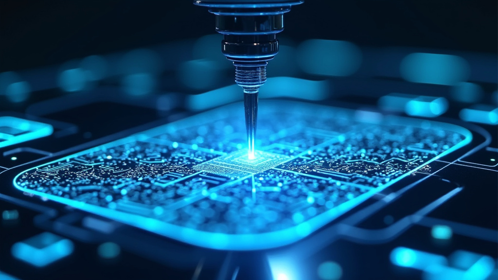
DNP’s new 10nm template is capable of patterning circuits for 1.4nm-class logic chips, essential for next-generation electronic devices. This advancement in Nanoimprint Technology directly addresses the increasing demand for miniaturization, critical for the performance of smartphones, data centers, and NAND flash memory. DNP has dedicated itself to advancing NIL since 2003, accumulating extensive expertise that underpins this latest development, which cleverly incorporates Self-Aligned Double Patterning (SADP) principles within its Nanoimprint Technology framework. The application of Nanoimprint Technology here is key for future chip production costs.
Addressing the EUV Lithography Challenge with Nanoimprint Technology
Extreme Ultraviolet (EUV) lithography is currently a dominant process in chipmaking, but it comes with substantial drawbacks. The enormous investment required for EUV production lines and its significant energy consumption pose considerable challenges, including an environmental burden. DNP’s Nanoimprint Technology offers a promising solution by providing a viable EUV lithography alternative that can partially replace EUV steps, thereby giving manufacturers more options. This is particularly beneficial for companies lacking direct access to EUV infrastructure. Crucially, this form of Nanoimprint Technology dramatically reduces energy consumption, potentially lowering power usage to one-tenth of that required by current exposure processes, thus paving the way for greener semiconductor manufacturing and a more sustainable chip production. This low energy lithography approach is a major benefit.
DNP’s Strategic Vision for Nanoimprint Technology
DNP has cultivated decades of experience and profound know-how in high-precision patterning, which has culminated in this impressive 10nm template. The company is strategically targeting mass production by 2027 and is actively engaging clients for evaluations of this transformative Nanoimprint Technology. DNP anticipates significant growth from its NIL business, projecting sales of 4 billion yen by fiscal year 2030. To showcase this innovation, DNP plans to exhibit its Nanoimprint Technology at SEMICON Japan 2025, held in Tokyo from December 17-19, 2025. This forward-thinking approach positions DNP’s Nanoimprint Technology as a key growth engine, aligning perfectly with Japan semiconductor innovation initiatives.
Industry Implications and Future Outlook for Nanoimprint Technology
The advantages of Nanoimprint Technology extend to significant cost savings and simplified manufacturing processes, which can lead to reduced overall chip production costs. Furthermore, its lower energy requirements are vital for achieving carbon neutrality goals within the industry. Japan is making concerted efforts to revitalize its semiconductor sector through new partnerships and governmental support, and DNP’s announcement represents a significant stride forward. This development highlights Japan’s continued innovation in advanced manufacturing. While EUV lithography will remain indispensable, Nanoimprint Technology presents a valuable complementary approach, enhancing manufacturing flexibility and potentially impacting chip costs. The industry is keenly observing the ongoing customer evaluations of this groundbreaking Nanoimprint Technology, including Dai Nippon Printing NIL capabilities.
Conclusion: The Promising Future of Nanoimprint Technology
DNP’s 10nm Nanoimprint Technology represents a major advancement, promising both reduced chip production costs and lower energy consumption. This innovative approach offers a vital alternative, potentially alleviating bottlenecks associated with EUV lithography and contributing to more efficient semiconductor manufacturing. The global semiconductor industry will be closely monitoring the progress of this Nanoimprint Technology towards mass production. This breakthrough has the potential to significantly reshape the future of chipmaking, underscoring Japan’s renewed strength and capabilities in this critical technological domain. The advancement of Nanoimprint Technology marks a new era for 10nm circuit patterning.